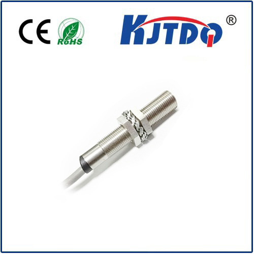
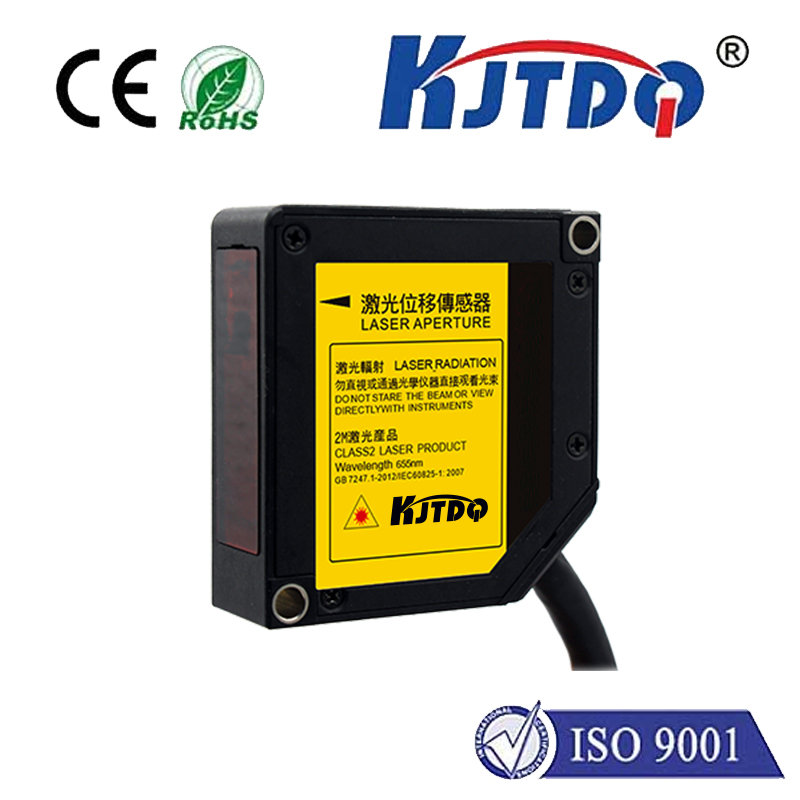
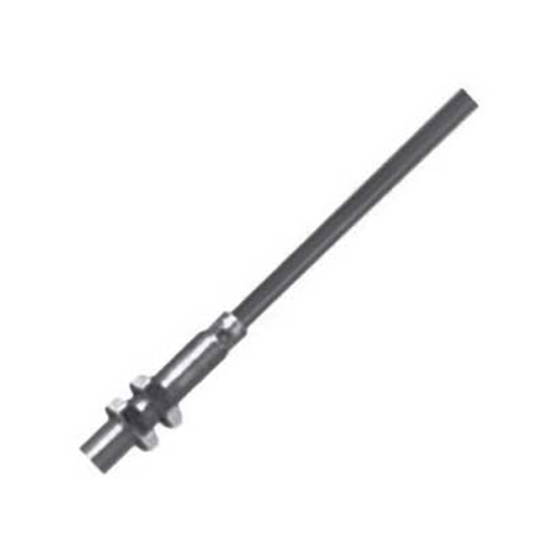
miniature optical sensor
- time:2025-08-13 17:42:58
- Нажмите:0
The Miniature Optical Sensor Revolution: How Tiny Light Detectors Are Transforming Industries
Imagine unlocking your smartphone with just a glance, even in glaring sunlight. Or picture a surgeon navigating the intricate pathways of the human body with an endoscope thinner than a grain of rice. Perhaps consider a factory where machines predict their own maintenance needs before a critical failure occurs. These seemingly disparate marvels share a common, invisible hero: the miniature optical sensor. These tiny, sophisticated devices, capable of detecting, measuring, and analyzing light in incredibly compact forms, are silently powering a wave of innovation across countless fields, shrinking possibilities while expanding capabilities.
So, what exactly is a miniature optical sensor? At its core, an optical sensor converts light (visible, infrared, ultraviolet) into an electrical signal. What defines its “miniature” status is the relentless drive towards extreme miniaturization, often leveraging advanced micro-fabrication techniques like MEMS (Micro-Electro-Mechanical Systems) and silicon photonics. Think millimeters or even micrometers in scale—small enough to fit unobtrusively into wearables, implantable medical devices, drones, smartphones, and dense industrial arrays. This dramatic reduction in size unlocks applications previously deemed impossible due to space, weight, or cost constraints.
The real power of these diminutive detectors lies in their pervasive impact. Let’s delve into some transformative applications:
- Consumer Electronics Revolution: Our daily tech companions rely heavily on these sensors. Miniature ambient light sensors automatically optimize smartphone screen brightness for battery life and readability. Proximity sensors prevent accidental screen touches during calls. Advanced time-of-flight (ToF) sensors map depth for stunning portrait-mode photos and enable immersive augmented reality experiences. Under-display fingerprint sensors utilize intricate optical patterns for secure, seamless unlocking. The relentless miniaturization allows these features to exist without compromising sleek device design.
- Medical Miracles in Miniature: The healthcare sector experiences profound benefits. Endoscopic capsules, swallowed by patients, contain miniature cameras and illumination systems, capturing detailed images of the gastrointestinal tract non-invasively. Tiny pulse oximeters integrated into smartwatches or rings continuously monitor blood oxygen levels. Implantable glucose monitors utilize miniature optical sensors for near-continuous diabetic monitoring. Lab-on-a-chip diagnostics use integrated optical components to detect pathogens or biomarkers rapidly using minute fluid samples, bringing sophisticated testing to point-of-care settings.
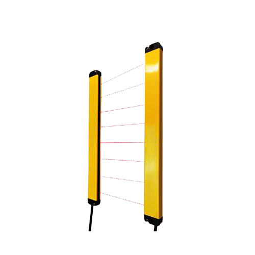
- Industrial Automation & Quality Control: On the factory floor, miniature optical sensors are workhorses. They perform high-speed, non-contact dimensional inspection of components on assembly lines with micron-level precision. Color sensors ensure product consistency. Miniature spectrometers, employing techniques like NIR (Near-Infrared) spectroscopy, analyze material composition in real-time for quality control in pharmaceuticals, food processing, and recycling. Vibration and tilt sensors based on optical principles provide crucial data for predictive maintenance of machinery.
- Environmental Monitoring & Sensing: Deploying networks of tiny, low-power sensors is revolutionizing environmental data collection. Miniature gas sensors using optical absorption principles monitor air quality for pollutants like CO2, methane, or NOx. Distributed fiber optic sensors, effectively strings of miniature sensing points, can detect leaks in pipelines, monitor structural health of bridges, or measure temperature variations over vast areas with incredible spatial resolution.
- Defense, Aerospace, and Robotics: In demanding environments, size, weight, and power (SWaP) are critical. Miniature optical sensors enable navigation (LIDAR), target designation, chemical detection, and structural health monitoring in drones, satellites, and robotic systems where every gram and cubic millimeter counts. Ruggedized versions withstand extreme temperatures, pressures, and vibrations.
How do these marvels of miniaturization work? The underlying principles are diverse, but miniaturization often hinges on advanced materials and fabrication:
- MEMS Technology: Allows the creation of tiny moving parts (like micromirrors or diaphragms) or waveguides on silicon chips. MEMS-based accelerometers and gyroscopes often use optical detection methods. Fabry-Perot interferometers can be miniaturized using MEMS for precise spectral analysis or pressure sensing.
- Silicon Photonics: This field integrates optical components (waveguides, modulators, detectors) directly onto silicon chips using standard semiconductor manufacturing processes. This enables complex optical circuits at a fraction of the size and cost of traditional bulk optics, paving the way for ultra-compact sensors and communication devices.
- Advanced Materials: Novel photonic materials, nanostructured surfaces (like metasurfaces for manipulating light), and specialized polymers enable new sensing mechanisms and enhanced performance within tiny footprints.
The advantages driving adoption are compelling:
- Unprecedented Size & Weight Reduction: Enables integration into spaces previously inaccessible.
- Enhanced Portability & Wearability: Vital for consumer electronics, health monitors, and field-deployable instruments.
- Lower Power Consumption: Crucial for battery-operated devices and large sensor networks.
- Potential for Mass Production & Cost Reduction: Leveraging semiconductor fabrication scales production and lowers unit costs significantly.
- Robustness: MEMS and integrated photonic devices can be highly resistant to shock and vibration compared to delicate traditional optics.
- New Functionality: Miniaturization enables novel sensing configurations and integration with other microsystems (like electronics and fluidics) on a single chip, creating powerful micro-total-analysis systems (μTAS).
Challenges remain, as with any frontier. Achieving high sensitivity and signal-to-noise ratios in such small packages can be difficult. Packaging these fragile micro-devices to protect them from the environment while allowing light access is complex. Calibration and maintaining performance consistency across vast production runs require sophisticated techniques. Designing effective, miniature light sources integrated with the sensors is also an ongoing area of development.
Looking ahead, the future for miniature optical sensors is dazzlingly bright. Continuous advancements in nanophotonics, quantum sensing, and artificial intelligence will push performance boundaries further. We anticipate sensors with single-photon sensitivity, capable of detecting specific molecules at ultra-low concentrations, embedded almost invisibly into everyday objects and infrastructure. Biodegradable sensors for temporary medical monitoring and increasingly sophisticated implantables are on the horizon. Further integration with edge computing will enable real-time, intelligent analysis right at the sensor node.
From the palm of your hand to the depths of the human body, from smart factories to environmental sentinels, miniature optical sensors are proving that the smallest components can drive the largest transformations. Their ability to perceive the world through light, packed into vanishingly small spaces, continues to redefine what’s technologically possible, shrinking devices while magnificently expanding the scope of human ingenuity and application. As fabrication techniques advance and novel optical principles are harnessed, their influence will only deepen, becoming even more ubiquitous and essential threads woven into the fabric of our technological future.