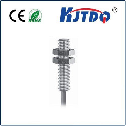
pnp proximity
- time:2025-06-20 03:00:59
- Нажмите:0
The Silent Architect: How PNP Proximity Shapes Circuit Performance and Reliability
In the intricate world of electronic design, success often hinges on elements beyond the schematic. The physical arrangement of components – where they sit on the board – plays a profound role in performance, stability, and longevity. While PNP transistors are fundamental building blocks, their effectiveness is significantly influenced by their proximity to critical circuit elements, especially other transistors and heat-generating components. Ignoring PNP proximity considerations can lead to subtle failures, frustrating debugging sessions, and compromised product reliability.
Beyond the Symbol: PNP Transistors in the Real World
Understanding Эффект близости starts with recalling the PNP transistor’s core function. As a current-controlled device, a PNP transistor conducts current from its emitter to its collector when a sufficient negative current flows out of its base relative to the emitter. This makes them invaluable for applications like high-side switching, current sourcing, level shifting, and specific amplification configurations.
However, transistors are not isolated islands. They exist in a physical environment on a Printed Circuit Board (PCB), subjected to:

- Thermal Gradients: Components generate heat. Adjacent components influence each other’s temperature.
- Electrical Noise: Switching currents, magnetic fields, and stray capacitance/inductance can couple signals unintentionally.
- Parasitic Effects: Physical closeness creates parasitic capacitance and inductance between traces and component leads.
Why PNP Proximity Matters: Key Considerations
The placement of a PNP transistor relative to other components isn’t arbitrary; it’s a crucial design parameter impacting several areas:
- Thermal Coupling and Stability:
- Heat Sharing: Placing a PNP transistor close to another power-dissipating component (like an NPN transistor, voltage regulator, or power resistor) means they share thermal energy. If the nearby device heats up, the PNP’s temperature rises.
- Impact on Characteristics: Transistor parameters like beta (hFE), saturation voltage (VCE(sat)), and leakage currents (ICBO, ICEO) are highly temperature-sensitive. An unintended temperature rise in the ПНП due to a proximal heat source can alter its operating point, gain, and even push it towards thermal runaway in power applications if base biasing isn’t carefully designed.
- Thermal Runaway Risk: PNP transistors can be susceptible to thermal runaway, especially in emitter-follower configurations or when driving heavy loads. Proximity to other heat sources exacerbates this risk by pushing the junction temperature higher, further reducing VBE (which increases base current for a fixed bias, leading to more collector current and more heat – a dangerous positive feedback loop).
- Electrical Noise and Crosstalk:
- Signal Integrity: Fast-switching digital circuits or high-frequency analog signals on nearby traces can induce unwanted voltages or currents into the PNP transistor’s base or collector circuits via parasitic capacitance or mutual inductance. This is especially critical if the ПНП is part of a sensitive analog stage or a precise current source.
- Ground Bounce: PNP transistors used for switching, particularly in high-side driver applications, can experience significant ground bounce if their emitter connections (which are often tied to the switched load) share long or inductive paths with sensitive logic ground returns. Proximity to ground planes and careful routing are vital.
- Symmetric Pairing (PNP-NPN):
- Matched Characteristics: In circuits requiring closely matched complementary pairs (e.g., push-pull output stages, certain amplifier types, precision current mirrors), placing the PNP transistor physically close to its complementary NPN counterpart is crucial. Proximity helps ensure both devices experience nearly identical thermal environments, minimizing offset voltages and drift due to temperature differences. This thermal tracking is essential for maintaining circuit balance and performance over temperature variations.
Designing for Optimal PNP Proximity
Managing Эффект близости requires deliberate PCB layout strategies:
- Thermal Management: Place PNP transistors away from major heat sources. If unavoidable, ensure adequate heatsinking specifically for the PNP, potentially isolating it thermally. Use thermal relief pads and consider copper pours connected to ground or appropriate planes to act as heat spreaders. For critical pairs, ensure thermal symmetry between PNP and NPN.
- Signal Isolation: Keep sensitive PNP base traces short and away from high-current switching paths or noisy digital lines. Use ground planes effectively to provide shielding. Route collector and emitter traces mindful of loop areas to minimize inductance.
- Power Routing: For high-side PNP switches, minimize the inductance between the emitter (connected to the positive supply) and the load. Place bulk decoupling capacitors physically close to the PNP’s collector connection (to the load) and the emitter connection (to the supply rail).
- Symmetry in Complementary Designs: When using complementary PNP/NPN pairs for outputs or mirrors, place them side-by-side, often sharing a common heatsink, to maximize thermal coupling between them. This promotes beta compensation and reduces thermal distortion.
Practical Applications Where Proximity is Paramount
Consider these scenarios where PNP placement significantly influences behavior:
- Linear Voltage Regulators: The pass transistor (often a PNP in certain topologies like low-dropout regulators - LDOs) dissipates substantial power. Its proximity to the error amplifier IC and feedback resistors is critical to avoid thermal gradients causing regulation errors. Thermal coupling between the pass transistor and a temperature-sensing element might even be intentionally designed in some cases.
- Audio Power Amplifiers: Output stages using complementary PNP/NPN pairs demand close proximity for thermal tracking. Uneven heating can lead to crossover distortion and degraded sound quality. Heatsink design must promote equal thermal resistance for both devices.
- Current Source/Sink Circuits: Precision current mirrors using PNP transistors rely on matched characteristics. Placing reference and mirror transistors in close proximity ensures they operate at the same temperature, maintaining current accuracy.
- Motor Drivers / Solenoid Drivers: PNP transistors used for high-side driving experience switching transients and ground bounce. Proximity to the load, flyback diodes, and low-inductance ground/power paths minimizes voltage spikes and EMI.
The Invisible Hand Guiding Circuit Behavior
PNP proximity is a fundamental, yet often overlooked, aspect of robust electronic design. It transcends the theoretical ideal captured in a schematic and grounds the circuit in the physical realities of heat, noise, and parasitic interactions. By consciously considering the thermal environment, potential noise sources, and the need for thermal matching, designers leverage placement as a powerful tool. Thoughtful management of PNP transistor proximity isn’t just about avoiding problems; it’s about unlocking higher reliability, improved performance stability, lower noise, and consistent operation across temperature variations – hallmarks of truly professional and dependable electronics. The silent architect of the layout profoundly shapes the circuit’s ultimate success.